|
|
|
previous page |
overall view |
next page
01 |
02 |
03 |
04 |
05 |
06 |
07 |
08 |
09 |
10 |
11 |
12 |
13 |
14 |
15 |
16 |
17 |
18 |
19 |
20 |
21 |
22 |
23 |
24 |
25 |
26 |
27 |
28 |
17 – Filling / Sealing of vias
The filling/sealing of plated through drill holes (vias) should prevent a run-off of solder during the soldering process or allow inspection in a vacuum adapter. The vias can be filled/sealed as follows:
• Covering with solder resist
• Via fillers
• Galvanic copper plating
• Plugging
17.1 – Covering with solder resist
The vias are covered during the production process using solder resist. To do this, they are not exposed to the solder resist. The disadvantage of this procedure: The vias are not sealed 100 % reliably as the solder resist hardens and can tear. In addition, they are not sealed vacuum tight. This procedure is frequently used in association with BGAs. However, chemical and moisture residues can lead to corrosion, surface wetting and solder problems. For this reason, this procedure cannot be recommended without reservation.
The better solution is to print the solder resist up to or on the annular ring. Solder resist openings should be +0,1 mm to the annular ring or by printing on the annular ring +0.15 mm to the drill.
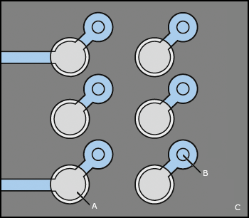
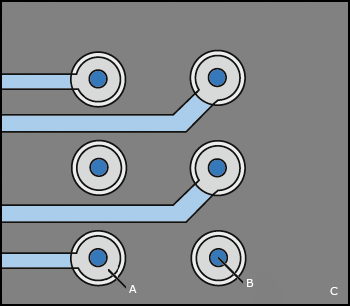
Fig.1: Typical pad-via arrangement in BGAs: The vias are introduced at a 45° angle to the pad and then covered using solder resist (dog-bone technique). |
|
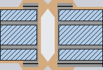
Fig.2: Sealed drill hole using solder resist
A SMD-Pads (Landing)
B Vias (drill hole)
C Solder resist |
17.2 – Via fillers
In order to seal vias vacuum-tight, it can be done using a single- or double-component varnish (in case of smaller vias, using solder resist varnish). For this, an additional film (Gerber film) is required for the vias involved. This procedure is not suitable for sealing vias in the pad, as it is not possible to solder onto these. However, it is possible to prevent the solder running through. Testing in a vacuum adapter is also possible.
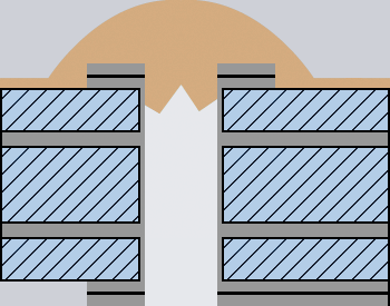
Fig.3: Via filler |
|
 |
17.3 – Galvanic copper plating
This sealing method is only possible in case of small diameters. To do this, the PCB is covered except for the relevant vias and these are galvanically copper plated. However, this procedure is very time consuming.
17.4 – Plugging PCBs
There are two plugging variants, depending on whether the pad surface has to be capable of being soldered or not. As an alternative to via fillers, normal vias can be plugged (HP = Hole Plugging). If, in order to save space, the via is placed directly in the pad, the surface must be metallically conductive in order to be able to solder on to it later on (HPL = hole-plugged land). To do this, the drill holes to be sealed must first identified, plated through and connected to the inner layers. In this, the entire PCB is copper plated. Then the plugging paste is applied. After curing, the PCB is resurfaced in order to recreate a flat surface. In this process, a few μm are also eroded. Then the remainder of the drill holes are introduced into the PCB and plated through . The PCB is again copper plated at the same time. Then the PCB is structured.
However, this procedure is problematical for blind vias, as air inclusions during the application of the plugging paste are possible. During the soldering process, this may lead to delamination.
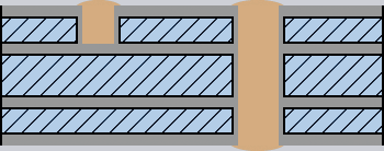
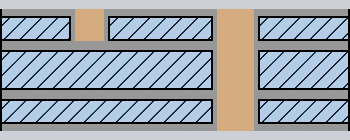
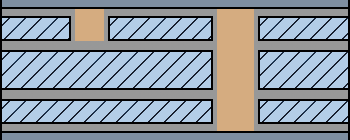
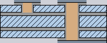
Work stages
1 – PCB drilled and through-plated
 |
|
2 – Drill holes filled with plugging paste
 |
3 – Grinded surface
 |
|
4 – Copper plated
 |
5 – Structured
 |
|
6 – PCB surface
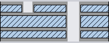
The space saving aspect comparing to the "dog-bone" technique is obviously.
A SMD-Pads (Landing)
B Vias (drill hole)
C Solder resist varnish |
17.5 – Advantages and disadvantages at a glance
A – Covering with solder resist
Advantages
• no additional costs
• flat surface
Disadvantages
• not vacuum-tight
• not for vias in pads
• unreliable
• possible inclusions of chemical residues and moisture
• wetting and soldering problems
Better: Printing the solder resist varnish onto the annular ring only
C – Sealed by copper plating
Advantages
• vacuum-tight
• electrically conducting
• vias possible in pads
Disadvantages
• cost-intensive (time-consuming)
• no flat surface
Parameters:
• PCB thickness max. 1,0 mm
• max. drill hole Ø 0,3 mm
• Aspect ratio max. 1:5 |
|
B – Via fillers
Advantages
• economical
• vacuum-tight
Disadvantages
• not for vias in pads
• no flat surface
• no finest-line circuits
Parameters: max. drill hole Ø 0,5 mm
Alternative: Plugging without further copper plating (HP)
D – Plugging (HPL)
Advantages
• vias possible in pads
• saves space on the PCB
• flat, sealed surface
Disadvantages
• cost-intensive, as numerous intermediate steps are required
• Risk of uneven copper erosion during resurfacing and associated
problems on structuring the PCB (particularly using technologies
< 0,15 mm)
• Plugging of blind vias is problematic
Parameters:
• Drill hole min. Ø 0,2 mm / max. Ø 0,5 mm
• min. width/gap of circuit-board tracks >125 µm
• Aspect ratio max. 1:8 |
|
|